Jeonghyun Park

Research Assistant
Seoul National University Quantum Information and Quantum Computing Lab

I graduated from the Department of Electrical and Computer Engineering at Seoul National University with a double major in Physics and designed and developed realtime quantum computer control system under professor Tae-hyun Kim. I had focused to design and implement RFSoC-based control system and mixed signal PCB. Currently, I aim to enhance my expertise in FPGA-related areas.

Jeonghyun Park

Email: alexist@snu.ac.kr

Publications

  1.  J. Park, M. Kim, Y. Cha, D. Chung, H. Shon, W. Lee, J. Kang, J. You, and T. Kim, “INQC:Integrated Trapped-Ion Quantum Computer Controller,” in preparation, 2025.
  2.  D. Chung, K. Choi, W. Lee, C. Kim, H. Shon, J. Park, B. Cho, K. Lee, S. Kim, and S. Yoo, “A silicon-based ion trap chip protected from semiconductor charging,” Quantum Sci. Technol., vol. 10, no. 3, p. 035014, 2025.
  3.  D. Chung, Y. Cha, H. Shon, J. Park, W. Lee, K. Lee, B. Cho, K. Choi, C. Kim, S. Yoo, S. Kim, U. Jeong, J. Kang, J. You, and T. Kim, “Radio-Frequency Pseudo-Null Induced by Light in an Ion Trap,” arXiv preprint arXiv:2504.13699, Apr. 2025.
  4.  S. Yu, K. Lee, S. Park, K. Kim, J. Goo, J. Park, and T. Kim, “Efficient quantum frequency conversion of ultra-violet single photons from a trapped ytterbium ion,” Appl. Phys. Lett., vol. 126, no. 8, Art. no. 084001, 2025.

FPGA Projects

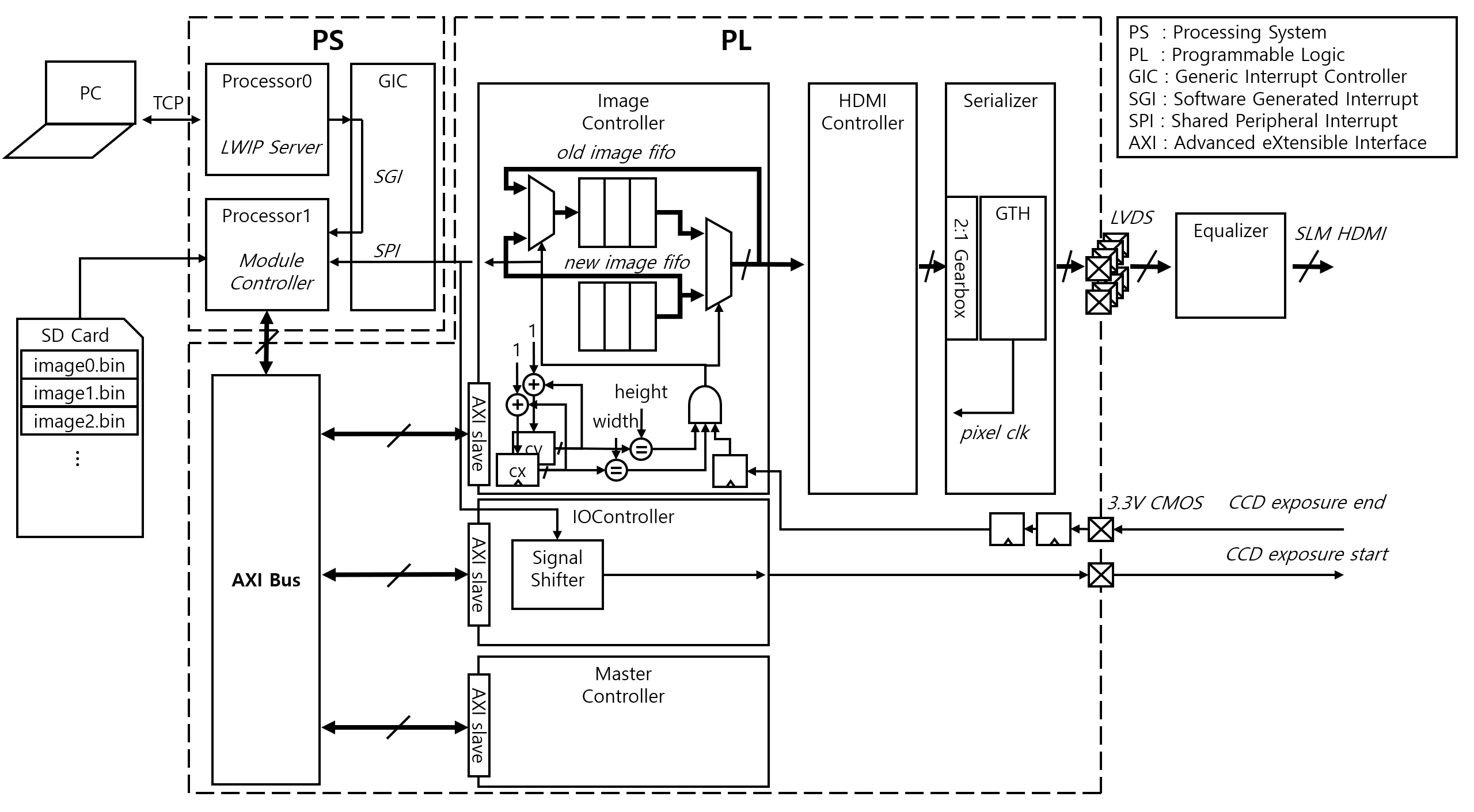
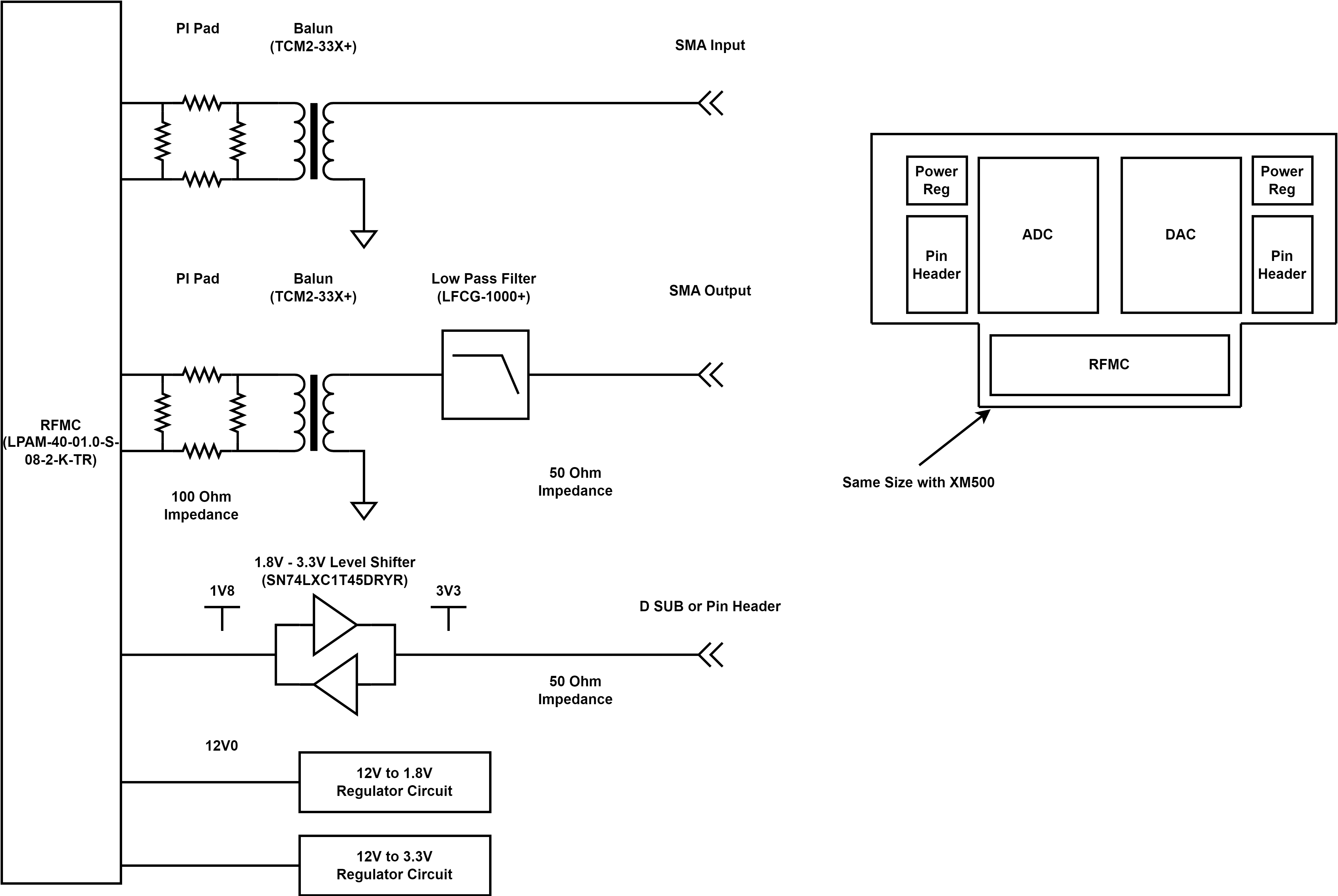
RFSoC-based Trapped-Ion Qauntum Computer Control System

Image1
Image2
Image3

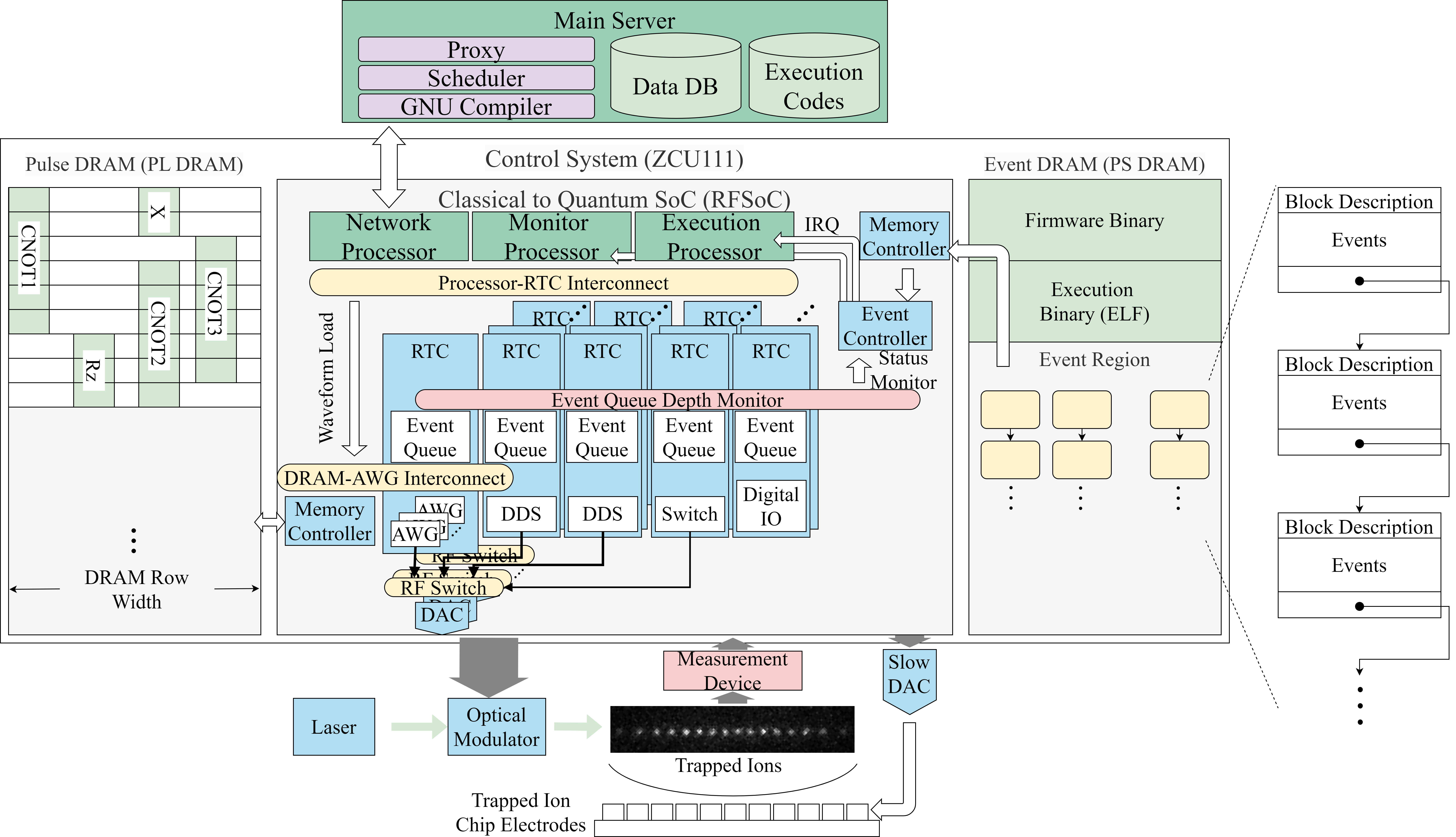
900 ns WCET latency with 1 channel, and 2.16 us with 8 channels, 4Gsamples, 1Gbps true-arb AWG with simultaneous ceaseless multi channel output with periodic DRAM refresh

Non-blocking DMA achieving 3.2GBps with simultaneous multiple independent modules enabling 5192 electrodes control

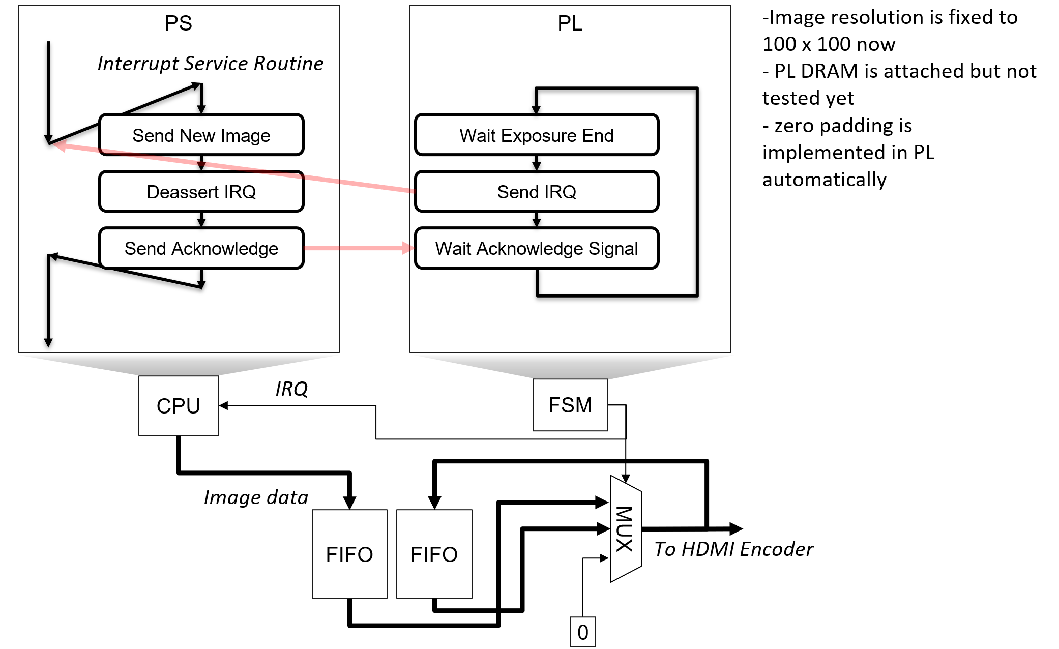
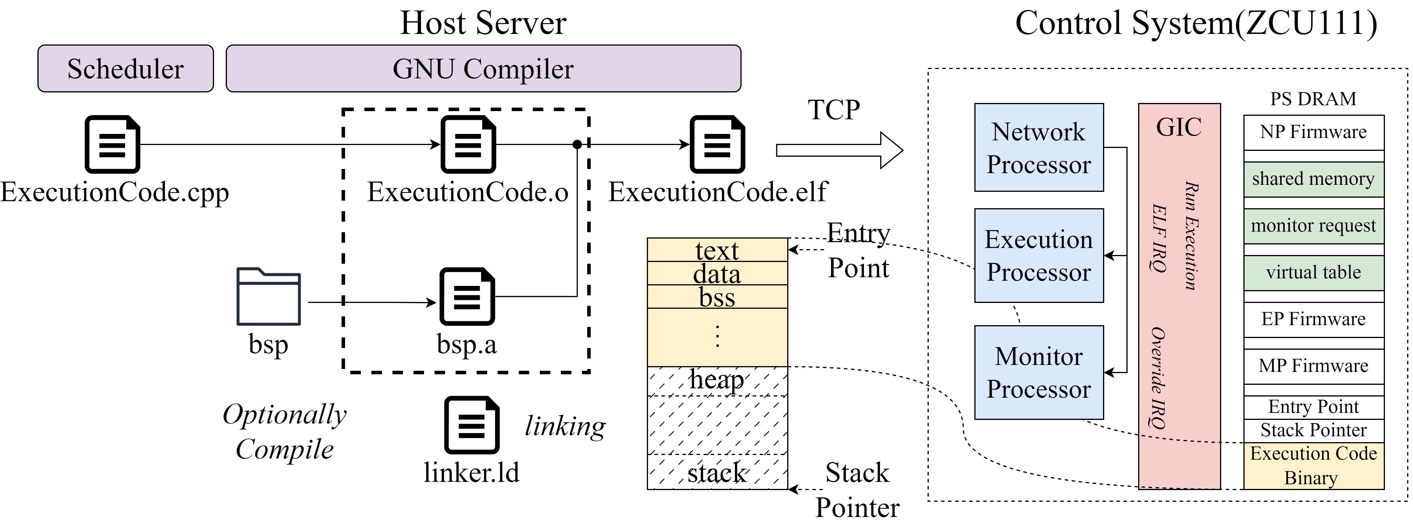
Realtime shuttling, measurement, baremetal server running C++ code in field are integrated on single chip

Json meta file based automatic FPGA project generation tool chain

Compile and transmit binary code and schedule experiment request, and conduct RPC from FPGA

Pulse optimization through ADAM algorithm and is verified with experiment

SLM Control, and Frame Grabber System

Image4
Image5
Image6

Realtime SLM control via DVI, Cameralink frame grabber

PCB Projects

RF Frontend

Image4
Image4
Image5
Image6

8-layer mixed signal daughter board achieving -20dB reflection, and 250dB isolated between digital interface controling pheripheral devices in realtime and analog region transmitting and filtering RF signal.

Low Noise DAC System

Image4
Image4
Image4

8-layer DAC board to implement realtime shuttling.

High Speed FMC Router

Image4
Image4

Daughter board which converts VITA57.1/4 FMC to EEM achieving 1Gbps differential signal transmission

Bidirectional LVDS to TTL

Image4
Image4

4-layer TTL-LVDS bidirectional convertor